|
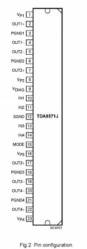
PINNING
|
|
SYMBOL
|
PIN
|
DESCRIPTION
|
|
Vpi
|
1
|
supply voltage 1
|
|
OUT1 +
|
2
|
output 1+
|
|
PGND1
|
3
|
power ground 1
|
|
OUT1-
|
4
|
output 1 -
|
|
OUT2-
|
5
|
output 2-
|
|
PGND2
|
6
|
power ground 2
|
|
OUT2+
|
7
|
output 2+
|
|
|
8
|
supply voltage 2
|
|
Vdiag
|
9
|
diagnostic output
|
|
IN1
|
10
|
input 1
|
|
IN2
|
11
|
input 2
|
|
SGND
|
12
|
signal ground
|
|
IN3
|
13
|
input 3
|
|
IN4
|
14
|
input 4
|
|
MODE
|
15
|
mode select switch input
|
|
Vp3
|
16
|
supply voltage 3
|
|
OUT3+
|
17
|
output 3+
|
|
PGND3
|
18
|
power ground 3
|
|
OUT3-
|
19
|
output 3-
|
|
OUT4-
|
20
|
output 4-
|
|
pGND4
|
21
|
power ground 4
|
|
OUT4+
|
22
|
output 4+
|
|
Vp4
|
23
|
supply voltage 4
|
FUNCTIONAL DESCRIPTION
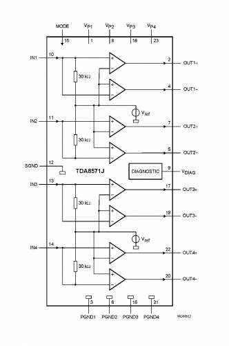
The TDA8571J contains four identical amplifiers which can be used for bridge applications. The gain of each amplifier is fixed at 34 dB.
Mode select switch (pin MODE)
• Standby: low supply current (<100 |iA)
• Mute: input signal suppressed
• Operating: normal on condition.
Since this pin has a low input current (<80 |iA), a low cost supply switch can be applied.
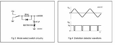
To avoid switch-on plops, it is advised to keep the amplifier in the mute mode during >150 ms (charging of the input capacitors at pins IN1, IN2, IN3 and IN4. When switching from standby to mute, the slope should be at least 18 V/s. This can be realized by:
• Microprocessor control
• External timing circuit (see Fig.3).
Diagnostic output (pin VDIAG)
Dynamic Distortion Detector (DDD)
At the onset of clipping of one or more output stages, the dynamic distortion detector becomes active and pin VDiAG goes LoW. This information can be used to drive a sound processor or DC volume control to attenuate the input signal and so limit the distortion. The output level of pin VDIAG is independent of the number of channels that are clipping (see Fig.4).
Short-circuit diagnostic
When a short-circuit occurs at one or more outputs to ground or to the supply voltage, the output stages are switched off until the short-circuit is removed and the device is switched on again, with a delay of approximately 10 ms after removal of the short-circuit. During this short-circuit condition, pin VDiAG is continuously LoW.
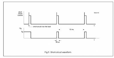
When a short-circuit occurs across the load of one or more channels, the output stages are switched off during approximately 10 ms. After that time it is checked during approximately 50 ms to determine whether the short-circuit is still present. Due to this duty cycle of 50 ms/10 ms the average current consumption during this short-circuit condition is very low.
During this short-circuit condition, pin VDiAG is LoW for 10 ms and HIGH for 50 ms (see Fig.5). The protection circuits of all channels are coupled. This means that if a short-circuit condition occurs in one of the channels, all channels are switched off. consequently, the power dissipation in any short-circuit condition is very low.
Temperature pre-warning
When the virtual junction temperature Tvj reaches 145 °C, pin VDIAG goes LOW.
Open-collector outputs
The diagnostic pin has an open-collector output, so more devices can be tied together. An external pull-up resistor is needed.
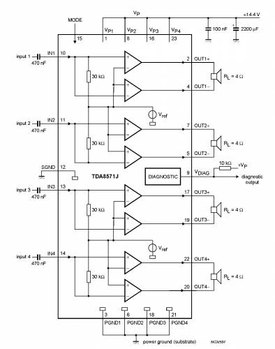
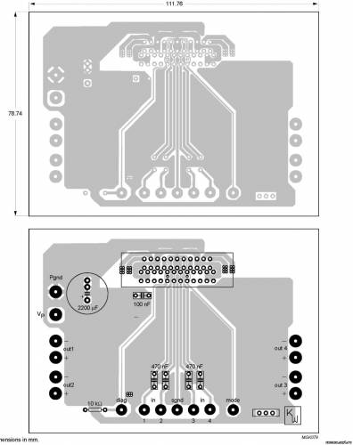
Special care must be taken in the PCB-layoutto separate pin Vdiag from the pins IN1, IN2, IN3and IN4to minimize the crosstalk between the clip output and the inputs.
To avoid switch-on plops, it is advised to keep the amplifier in the mute mode during a period of > 150 ms (charging the input capacitors at pins IN1, IN2, IN3 and IN4).

SOLDERING
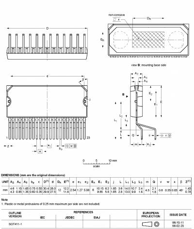
Introduction to soldering through-hole mount packages
This text gives a brief insight to wave, dip and manual soldering. A more in-depth account of soldering ICs can be found in our "Data Handbook IC26; Integrated Circuit Packages" (document order number 9398 652 90011).
Wave soldering is the preferred method for mounting of through-hole mount IC packages on a printed-circuit board.
Soldering by dipping or by solder wave
The maximum permissible temperature of the solder is 260 °C; solder at this temperature must not be in contact with the joints for more than 5 seconds.
The total contact time of successive solderwaves must not exceed 5 seconds.
The device may be mounted up to the seating plane, but the temperature of the plastic body must not exceed the specified maximum storage temperature (Tstg(max)). If the printed-circuit board has been pre-heated, forced cooling may be necessary immediately after soldering to keep the temperature within the permissible limit.
Manual soldering
Apply the soldering iron (24 V or less) to the lead(s) of the package, either below the seating plane or not more than 2 mm above it. If the temperature of the soldering iron bit is less than 300 °C it may remain in contact for up to 10 seconds. If the bit temperature is between 300 and 400 °C, contact may be up to 5 seconds.

